|
| Crystallographic Texture |
|
|
Individual grain orientation measurement in the TEM from The first Transmission [1] as well as Backscatter [2] Kikuchi Patterns (later named TKP and BKP) were published 1928 in the same volume of Proceedings Imperial Academy of Japan. During the next decades physicists focused their experimental work preferably on Transmission Kikuchi Diffraction (TKD) because of instrument-based reasons. Backscatter Kikuchi diffraction gained little attraction in material science, whereas the so-called RHEED technique (Reflection High Energy Electron diffraction at almost grazing incidence of the primary beam) found some applications in solid state physics. After the SEM became common place in the labs Backscatter Kikuchi Diffraction (BKD) in the SEM, then named Electron Backscatter Diffraction (EBSD), received attention of material scientists for texture analysis. For details please visit http://www.ebsd.info. In the TEM the diffraction patterns are either acquired with a CCD camera 1 placed on-axis at the bottom of the microscope column, or with a retractable CCD camera 2 above the viewing screen which is mounted on the standard side-entry flange. A budget-friendly alternative is the acquisition of the patterns from a phosphor screen with a CCD camera 3 through a window from outside (Fig. 1) [3, 4].
Projection chamber of a Philips 430 TEM with three positions of CCD cameras A circular continuous density filter in the optical path is of advantage to equalize the steep drop of intensity from the blooming primary beam spot to the dim marginal area. Pattern intensity is of minor concern in TKD with a TEM. The patterns should cover a large angular range and be undistorted. These requirements limit TKD orientation mapping to the use of a TEM with a condenser objective lens and microbeam diffraction facility such as for instance the Philips CM series, respectively FEI TEM. For automated mapping [4] a computer controlled scan of the beam spot is implemented. Preparation of freestanding, flat and transparent thin samples from the bulk for TKD in the TEM or SEM is often tedious. It is a difficult task in particular when the sample is non-noble, heavily deformed, tends to reactions and etch pitting or contains several phases. The study of thin films is often questionable when conclusions are to be drawn on properties of bulk materials. Residual stress in the foil may lead to rotations of grains as well as nihilation of dislocations at the surface. Dynamic investigations such as heating stage or tensile stage experiments are less meaningful. TKD, however, is an excellent tool to inspect microstructure and texture of "natural" thin films, for instance of vacuum ecaporated or sputter coated films, surface coatings, or cross sections through stapled layers made uncovered by FIBing. Current research with TKD focuses on nanoscale materials or severely plastically deformed materials, which may show drastic changes in properties with often unexpected results as compared to conventionally manufactured materials. Buckled foils, almost unavoidable due to preparation and local stress, are in many cases not a real problem for the study of polycrystals or single crystals with the TEM. The metallurgist uses a TEM typically to investigate very small sample areas, e.g. for dislocation or phase analysis, special grain boundaries, lattice misfits, high-resolution lattice imaging and Burgers vector analysis [5]. The operator can thus select a small area with no bend contours and other flaws in the images to produce trustworthy crystal orientation maps. With TKD in the SEM, on the contrary, we usually want to study large sample areas containing many grains. Then bent foils may be a problem since the orientation data are spoiled by the overlay of geometrical wrinkling. With fine grain material the false orientations are not obviously apparent by deviating colors or shades in the crystal orientation maps. However, pole figures and ODF are unduly smeared up by topography. Interpretation of texture may be misleading.
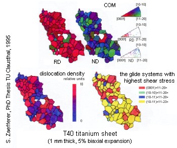
Misorientation data across abutting grain boundaries are not seriously affected by foil buckling. EBSD in the SEM is carried out on bulk samples. The main requirements are a flat and clean surface free from preparation artifacts such as undue deformation, reaction layers or phase-selective etch. Examples of Crystal Orientation Maps (COM) from
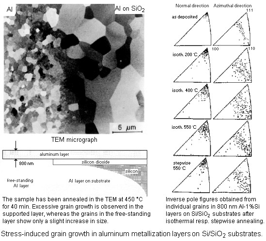
Application of the transmission Kikuchi technique to stress-induced grain growth in thin films. ___________ You can find a detailed survey over individual grain orientation measurement with the TEM and 56 references in: |

|